Building the Chiplet Interconnect for AI Infrastructure
No Interposers Required
Wire abundant interfaces (1K / 0.25 mm**2)
Up to 50% reduction in Chiplet Die Area
50x smaller, 10x less energy/bit, 10x lower upfront cost
No Interposers Required
Wire abundant interfaces (1K / 0.25 mm**2)
Up to 50% reduction in Chiplet Die Area
50x smaller, 10x less energy/bit, 10x lower upfront cost
| Bridgelet | Direct Chiplet Input/Output (DCIO) | |||||
|---|---|---|---|---|---|---|
| Features | Benefits | Features | Benefits | Disaggregates system I/O from memory functions | Allows chiplet reuse within or across product families | Ultra Short Reach (<500µ) | Lower power and area; Higher performance |
| Die scale interconnect (sub-micron) | Higher density and performance; Lower power | Protocol Agnostic | One PHY for multiple protocols | |||
| Enables “Beyond the Reticle” constraint | Extend SoC designs | Die Scale Interconnect (sub-micron) | Higher density and performance; Lower power | |||
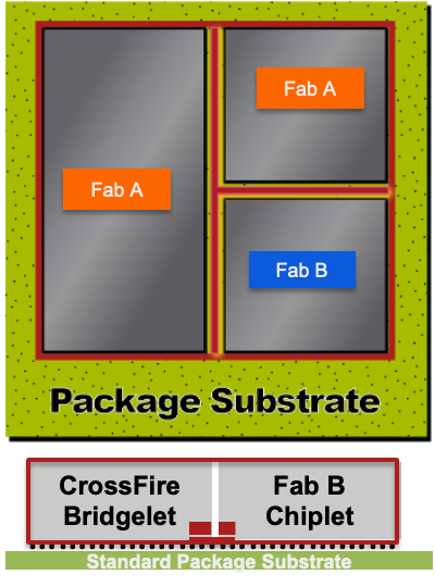
CrossFire’s Bridgelet products provide the Chiplet to Chiplet interconnect currently provided by Interposers, but without the cost, complexity or availability limitations. Depending on system requirements, Bridgelets can be either passive or active. Bridgelets are compatible with industry standard Die to Die (D2D) PHY’s such as UCIe and Bunch of Wires (BoW), as well as proprietary and non-standard D2D solutions such as Ultra Short Reach SerDes.
Current D2D PHYs contain unnecessary and burdensome features such as needlessly robust Electrostatic Discharge (ESD) protection, large pad sizes required by Interposer assembly techniques, overpowered Input / Output drivers, and signal conditioning circuitry. To address these pain points, CrossFire developed a Chiplet Input / Output solution called Direct Chiplet Input / Output or DCIO. This solution is compatible with standard link layers such as UCIe and BoW. Additionally, implementations such as UCIe over DCIO can provide 10x lower power, 10x lower cost, and 10x higher density than competing solutions.
CrossFire’s proprietary OmniDie capability provides for the physical integration of Chiplets and other die into a conjoined group of die – enabling the “SuperChip”. An OmniDie is typically mounted directly onto a package substrate, minimizing the requirement for costly Advanced Packaging solutions to integrate Chiplets